Long, long ago… In a workshop far away…
Recently, I’ve seen quite a few search hits and even an enquiry regarding the 400-LED dual-trace oscilloscope that I briefly mentioned on my History page. With renewed enthusiasm therefore, let’s take a trip down history lane and see what I was doing back in 1990!


PROJECT REPORT
Subject: Dual-Trace Oscilloscope Design and Construction
Period: 7/90 – 10/90
Submitted to: Mr R. Young, Physics Department
Project Designed and Constructed by: [Aaron] (present-day Oscilloclock.com)
PROLOGUE
When students studying Grade Twelve Physics began a unit on Electronics during the third term of the year, I became increasingly involved with the apparatus used by the teacher, Mr. R. Young. As I was already familiar with most of the material set out in the unit, I often helped Mr Young construct test circuits and/or set up equipment as teaching aids. In this context, I soon came to know the oscilloscope to a great extent. Having been an electronics hobbyist for the last twelve years, I was well aware of the functions of the oscilloscope, and to use it quickly became second nature to me. I was amazed at the detail of the information which the instrument gives the user about a circuit, and felt inclined to construct my own.
I knew of a very simple design idea for an oscilloscope, which was detailed
in the Engineer’s Notebook – A Handbook of Integrated Circuit Applications, published in 1980. I found a much more recent, yet almost identical circuit in Electronics Australia, July 1990.
I was not satisfied in the least with the idea of having a 100-LED matrix, simple oscillator, no amplification of input, and only a single-trace circuit. From this unsatisfaction swelled a 23-IC circuit which took between 50 and 90 hours to design and construct, and an immense cost of over A$270.
Needless to say, the project was not worth the money spent on it in terms of its efficiency, its lack of frills, and its amateurisms. However, I can say with no hesitation that the knowledge and experience which I gained during the design and construction period will stand me in good stead in later years, and to gain it was worth every single cent.
Aaron
THE INITIAL CIRCUIT
The basic circuit of the oscilloscope, and the one from which I started, is shown below. As described in the text, the 4017 IC is a decade counter, arranged to turn on each column of LEDS sequentially according to the clock pulses fed to it by the 555 circuit. The LM3916 is a dot/bar display driver, which turns on columns according to the signal input level. The LM3916 is a logarithmic driver, so it was necessary to use an LM3914 in the prototypes, a linear driver.
(Editor’s note: I wasn’t able to find my EA July 1990 issue, but you can find a roughly identical circuit here.)
THE FINAL CIRCUIT

THE DESIGN PROCESS
THE HORIZONTAL OUTPUT CIRCUITRY
The first stage of development was to cascade two 4017’s together to give a twenty-LED horizontal row. A rudimentary 4011 oscillator was used as a temporary oscillator, as the circuit for this section was developed.
My first attempt resulted in two 4017’s cascaded using a 4013 flip-flop. The flip-flop would control the ENABLE inputs of the 4017’s such that only one 4017 could be operating at once. This arrangement was unsatisfactory because when one 4017 was operating, the other allowed its No. 1 LED to REMAIN ON while the chip was halted.
Three to four weeks were spent on finding a solution to this problem, which was solved by the addition of IC12 and IC13. These NAND gates control the No. 1 LED of each 4017. The No. 1 LED of one 4017 is only allowed to turn on if the other 4017 is halted, and it is that LED’S turn to come on. In practice, it was not simple to created the circuit which would do so, and in the end 4 NAND gates were required for each 4017.
At this stage, the twenty LEDS would light from the start of one 4017 to the end of the other, and return for another cycle. Next to be added was the inclusion of a trigger input, to allow the LED count to reset back to the first LED (column). This was achieved by halting the 4013 and its driver 4017, as well as resetting IC10 and IC11 when the input to IC14(c) was held high. When triggered, the No. 1 LED of IC10 remains on – FAULT NO. 1.
THE VERTICAL OUTPUT CIRCUITRY
The next most vital step was to develop an arrangement of LM3914 display drivers which would produce a 20-LED display, with an overload LED.
Firstly, two LM3914’s were cascaded by stringing their internal voltage dividers in series (connecting pin 6 of the first to pin 4 of the second), and tying the ends of the combined voltage divider string to earth (pin 4 of the first) and to the positive supply (pin 6 of the second). In this case, with a supply voltage of 8 V, sensitivity was 8/20th Volts per LED. However, the top order LED of an LM3914 would remain on even with saturation. This problem was solved by linking 22 k resistors between pin 11 and supply. This caused an internal feedback loop to be disengaged.
At this stage, an overvoltage indicator was added by the addition of another LM3914 into the voltage divider string, making the first two LM3914’s turn their lowermost LED on at 0 V and 2 2/3 V respectively. Sensitivity was now 8/15 V per LED.
The LM3914 ICs have both dot and bar modes, and I decided that it would be to my advantage to use these modes to create a shading effect. For any LM3914, if pin 9 is connected to supply, it is put in bar mode. If pin 9 is connected to pin 1 of the next IC, it is put in dot mode. For a standard view, all 3 LM3914’s are in dot mode. For positive shading, the first and last LM3914 are in dot mode. For full shading, only the last is in dot mode. The CH1 MODE and CH2 MODE switches cater for these possibilities.
The last LM3914 is always in bar mode. so that the OVERVOLT Led will always light for any voltage over 5 1/3 V.
THE DISPLAY
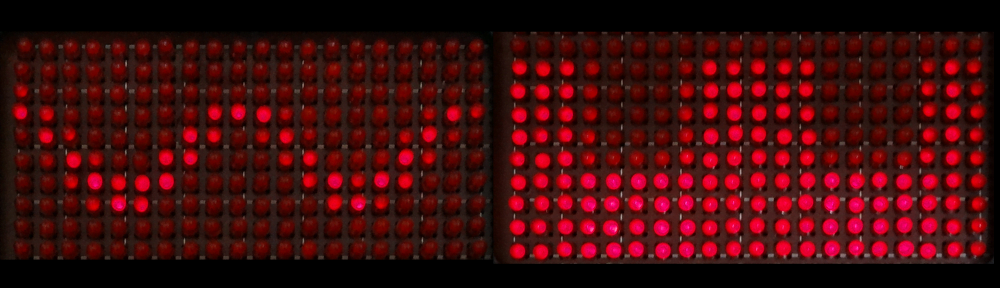
To form the display, 400 LED’s were connected in a matrix of 20 x 20, with common anodes in each column, and common cathodes in each row. 3 mm LED’s were used, mounted on a perfboard.
After soldering the 400 Leds in, the matrix was connected to the horizontal and vertical circuitry, and the prototype vas operational!
THE VERTICAL DRIVER CIRCUITRY
I desired a very low V per LED value, maybe 1/20 V for ease of calibration.
It was therefore necessary to add operational amplifiers to the inputs of each channel’s LM3914’s. Centering was achieved by biassing the -ve inputs of the op amps to be somewhat +ve. The +ve inputs of the op amps were biassed to +5 V by IC23, such that all input signals were with respect to +5 V.
This +5 V was the common.
The V/DIV switches switch the inputs to the ‘scope back and forth along voltage dividers to give a range of input levels.
THE TIMEBASE
Various attempts at producing a timebase oscillator which would be accurate and easy to tune resulted in little success. The simplest and cheapest arrangement found was to have a tuneable high-frequency oscillator, operating from about 2 MHz to about 200 kHz, and to divide this clock output by 10 any number of times. This division was done using 4017’s configured as divide-by-ten counters.
The major problem with an arrangement such as this is that the adjustments will be minimal on the lowest frequency range, compared to those on the highest frequency range. Thus it is easier to tune to a 50 Hz sine wave than to a 5 kHz sine wave. This is a significant problem, but time and financial constraints forced me to merely add in provisions for an external timebase, and install the timebase circuit as it was.

TRIGGER CIRCUITRY
To achieve a triggered display of a waveform, the horizontal ‘movement’ of the dot across the screen needed to be halted IF the left-most column was activated and the input waveform was NOT yet at a specific point in its period.
This specific point vas chosen as the most +ve peak of the waveform. In other words, if the first column was activated, and the waveform was not yet at its peak, then the horizontal movement must be halted until it gets there. This will ensure a somewhat stabilized waveform on the screen.
When the trigger circuit is switched in, IC16(c) and (d) amplify the waveform present at the inputs to the LM3914’s. The waveform is then buffered and rectified, and its peak voltage stored in the 33 uF capacitor. This voltage is buffered and appliers at pin 8. In IC16(a), this peak voltage is compared at all times to the AC signal at the LM3914’s, and when they are equal (when the waveform is at its peak), pin 1 goes high.
ICl6(b) is used to determine whether the current column activated is column i. If so, pin 7 goes low. We require the trigger to operated when column 1 is activated and the waveform is NOT at its peak. Hence the outputs at pin 1 and pin 7 are inverted by IC15(a) and (b), and ANDed to give the necessary triggering pulses.
The shortcomings with this arrangement lie in ICl6(b) and its underlying principle. The output of IC12(b) when column 1 is ‘on’ is not 8 V. Indeed, it lies between 0.01 and 3 V, for it is instantaneous and it drives a heavy load (the LED’s are operating at 15-20 ma current). IC16(b) compares this voltage with the voltage set by the l8k and 22 ohm resistors, about 0.01 V.
The trouble is that at higher and higher frequencies, the voltage at IC12(b) becomes more and more instantaneous, with lower frequency-compensated voltages.
Thus the reference voltage of 0.01 V is no longer valid, for it must be lower to cater for lower and lower voltages.
It is impractical to do so, however, so the circuit was installed as it was. The net result is that at higher and higher frequencies, the trigger circuitry ceases to function because it senses that column is never ‘on’.
This is FAULT No. 2.
SUPPLY CIRCUITS
The mains supply consists of a 6 V RMS mains transformer, driving a simple voltage doubler rectifier circuit. The output is filtered rather crudely using the 1000 uF capacitor. When the power lead is not plugged into the battery pack jack, then the unit runs from 11 – 18 V batteries. Otherwise, power is taken from the mains supply.
Input voltage is regulated by the 7808 8 V regulator, IC1. The battery indicator operates by comparing a voltage taken from the unregulated supply input (adjusted by the 50 k trimpot) with a voltage taken from the regulated supply, via the two 15 K resistors (4 V). The comparison is made by IC2(c) and (d). Either the red or green segment of the tri-state LED is on at any one time, according to the status of the comparison.
CONSTRUCTION
After each section of the circuit had been designed and perfected on a bread- board, they were then transferred in their final form onto matrixboards, for later amalgamation. In the end, seven separate matrixboards were used, including that used for the LED’s.

The cabinet was bought unlabelled and undrilled from Tandy Electronics for $20. An entire 7-hour day was spent in drilling the necessary holes and making the cutout for the screen. A further day was spent in labelling the panel, a tedious job of transferring rub-on letters onto the chassis.
The cabinet was then sprayed with two coats of photographic lacquer.

Front-panel controls were mounted first, with most still connected to their respective boards. Wiring was then laid neatly along the inner perimeters of the cabinet, for the ease of future service. Side-panel controls and sockets were mounted next, and wired in. All boards were arranged such that they could ‘hinge’ out on their connecting cables for ease of inspection or service. Only the multiplier, oscillator, and trigger boards were fixed in place rigidly. Other boards were expected to remain in place with the pressure applied on them with the case closed.
It was found that the sensitivity of the vertical driver circuitry was such that electromagnetic radiation from the oscillator and multiplier boards was enough to cause a deflection on the screen. It was necessary to earth the entire chassis (to +5 V), as well as shielding each PCB individually.
This was achieved by covering aluminium foil with electrical tape, folding this around each board, and connecting the internal foil to either earth, +5 V or supply.
The actual construction of the unit took only about 20 to 25 hours in total, compared with at least 40 for the actual design and theory work. A wooden instrument case was donated by the Manual Arts Department, which I very gratefully used to house the oscilloscope, a digital multimeter, a gas soldering iron, and miscellaneous tools.
The oscilloscope was mounted on a small, thin board which hinges out to a near-vertical position. A rod is pushed into any of a series of holes as a backrest, to allow a wide range of viewing ankles. When operating, the top of the case may be brought down on top of the oscilloscope unit, shielding the screen from the sun to make for greater visibility. The oscilloscope may be removed by removing a single rubber strut from its chassis.
COMMENTS AND IMPROVEMENT SUGGESTIONS
The maximum frequency of the wave which can be displayed across the entire screen in one period is only about 800 kHz using the circuit developed. The maximum theoretically possible with the components used is only about 900 kHz. Thus, the oscilloscope has a maximum useful frequency limit of about 3 MHz, which is a respectable standard for a homemade unit.
Maximum sensitivity is 31.25 mv per LED (division), with attenuation ranging from zero to infinite. Input impedance ranges from 250K to 8M ohms. Displayed waveforms are generally clear and distinct, at least as much as can be expected for such a low resolution device.
Areas which could be given much attention to are marked throughout this text with FAULT NO. X. These include the trigger circuitry (greater bandwidth necessary), the timebase (range control linearity over multiplier settings), and, most obviously, screen resolution.
HOWEVER, the time and expense already spent on the project have decreed that it is best to stop with the circuit as it is. It would hardly be worth improving the circuit or resolution at the cost of an extra $100 when a complete CRO can be bought for $399 (granted, it would not be dual-trace!).
As mentioned previously, I am satisfied with the oscilloscope and it will prove to be a useful test and design instrument in later projects. My sincere thanks go to Mr Young, who allowed me to access the school instruments, which were the sources of inspiration for me to build this project.