In the previous post, we looked at the Garmin 18x LVC “puck”. We talked about a particularly insidious issue that affected [Andrew] – both of his GPS units. And we saw that Oscilloclock owners really need to be able to update the firmware in these units.

We introduced the Oscilloclock Garmin 18x USB Adapter, that allows an Oscilloclock owner to connect their puck to a PC to enable the firmware upgrade.
In this post, we’ll take a look at the design of the Oscilloclock Garmin 18x USB Adapter. It wasn’t GPS satellite launcher (a.k.a. ‘rocket’) science, but it certainly wasn’t as straightforward as it might seem!
The Garmin 18x LVC electrical interface
Referencing the manual, the Garmin 18x series comes in 3 basic interface variations:
- USB – USB 1.x interface, with a USB(-A) connector to plug into a PC
- PC – RS-232 serial interface*, with a DB9 connector to plug into a PC, and a massive cigarette lighter adapter plug to obtain power
- LVC – RS-232 serial interface*, with no connector – for wiring into a device


For our Oscilloclocks, we use the LVC variation and fit an attractive custom connector solution, avoiding the PC variation with its venerable, utilitarian, and aesthetically unpleasant DB-9 connector and cigarette lighter plug combo. (We may buck the trend one day and intentionally fit such sockets into that special retro clock build – who knows?!)
* Astute readers noticed the earlier asterisks. PC and LVC units are not quite true RS-232; their output voltage swings between 0V and +5V. Not so with devices having true RS-232 interfaces! A swing from -25V to +25V is legal and also lethal for any unsuspecting microcontroller. In the Oscilloclock design, we take advantage of Garmin’s voltage range cap to avoid having additional circuitry to adjust voltage levels.
Interfacing the 18x LVC to a PC
To upgrade the GPS firmware, the 18x LVC needs to connect nicely to a PC. But [Andrew] is an Oscilloclock Owner. He deserves more than just a good electrical connection. The interface also must be elegant and aesthetically pleasing, lightweight (for shipping), and easy to build. And – most of all – it has to be interesting enough to write a blog series about!

We can start with Figure 1 in the manual, which describes the most basic interface hook-up possible.
This interconnection option assumes two things: the PC has a DB-9 serial port, and there is a power source.
If we extend this option slightly, to take power from the PC’s USB port, we arrive at this:

But who has a PC with a serial port in this day and age? Fortunately, there are plenty of RS232 Serial-to-USB converters out there – cheap and reliable! And we arrive at this:

Electrically, this is fine and dandy. And the build cost is not too bad. But it’s not so elegant. We can do so much more! First, we can get rid of the 2nd USB connector, by hacking into the serial-USB adapter, and tapping the power out from there:


While this solves the problem of the power, it’s NOT elegant, NOT pleasant to look at, and NOT really reliable.
Oscilloclock owners should not own junk, regardless of how ‘clever’ the solution is.
What we really want is an RS232 to USB adapter unit that provides both power and signal right out of the box. No hacking!

Sadly, there are no off the shelf RS232 to USB adapters that don’t have a DB9 socket embedded in them. We’d have to hack. Or, we could design our own elegant unit, from the PCB on up. (We’re good at that, but it would be a large effort to go to…)
A new idea – TTL Serial!
Is there another option? Well, in the past decade or two, TTL serial, another type of serial interface standard, has come into very common use. There are heaps of TTL serial to USB adapters on the market, and none of them have large clunky DB9 sockets built in!
It turns out the TTL serial electrical interface is similar to RS-232 serial, with two differences:
- TTL serial sports microcontroller-friendly voltage levels – i.e. between 0V and a capped upper limit such as 3.3V or 5V.
- TTL serial uses intuitive signal polarity. A ‘low’ is represented by a low voltage, near 0V. In RS-232, however signals are inverted – ‘low’ is a +ve voltage, and ‘high’ is a -ve voltage.
On the first point, recall from an earlier footnote that the 18x LVC’s voltage swing is from 0 to supply voltage. This is actually in line with TTL serial. Nice!
But the second point is almost certainly why Garmin explicitly mention “RS-232 polarity” in the GPS 18x manual. They don’t want anyone using the 18x LVC to get it wrong:

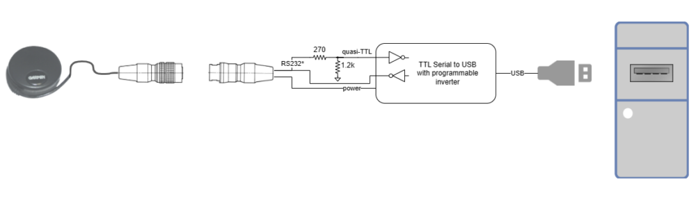
Since the 18x LVC features RS-232 polarity signals, we design around this. For example, the Oscilloclock Control Board features inverters on the receive and transmit lines, to allow the microcontrollers to process the signals as if there were TTL serial:

Hey, wait a minute – if the 18x LVC is pretty much TTL serial compatible from a voltage standpoint, and it’s just a matter of signal inversion, then we could use one of many TTL serial to USB adapters on the market! Some of them look very pleasant indeed. We would just need to invert the signals. And thus we have the next design:

Programmable Inversion
Doing just a little bit more research, it turns out that many of the common TTL serial to USB adapters on the market use a chip from FTDI, a company that specialises in USB bridging (interfacing) solutions. And the great news here is that FTDI chips support programmable inversion. We can eliminate the extra hardware needed to invert the signals!

FTDI provides a nifty app to program these inversion settings. We’ll see it in action soon.
CMOS vs TTL, and noisy signals
We noted earlier that the Garmin 18x LVC output swings between 0 and 5V. This is the same voltage range that TTL serial expects. All good, right? No, there is a slight difference that we may need to account for, to make the interface reliable.
The LVC has a CMOS output, while the FTDI chips have a TTL input. These acronyms describe the circuit configuration inside logic gates, and they differ in terms of the voltage ranges that logic gates deem acceptable when interpreting “low” vs. “high” signal levels.


There is an excellent writeup here that explains the difference in signal voltage levels in detail. The article explains that in an ideal world, connecting a CMOS output directly to a TTL input is not an issue. But our world is not ideal, and in our case we have a problem: TTL inputs are not very tolerant to noise compared to CMOS inputs.
And in reality, the LVC’s output signal is noisy! There are many possible factors:
- The 5m-long cable may be lossy
- The 5m-long cable may be picking up stray signals (like an antenna)
- The LVC designers probably expected us to process signals with an RS232 interface or directly connect to a microcontroller – both having (less noise-sensitive) CMOS inputs

I’ll spare you an oscilloscope screenshot, but the concept is illustrated to the extreme in this figure. The actual voltage (in green) has AC noise superimposed, and is not even able to keep up with the small burst in the middle.
Probably the most serious ramification of this for us is that the voltage can actually exceed 5V. This is a big no-no for standard 5V TTL logic, where (unlike CMOS) the maximum input is a strict 5V. Behaviour is undefined or erratic above that level.
There are some impressive ways out there to solve this – for example, introducing a CMOS buffer right in front of the TTL gate. But our goal is to keep it simple yet reliable. How about a simple resistive voltage divider?

This reduces the risk of exceeding 5V by dropping the input voltage by about 20%. It also subdues stray signals picked up by the cable, by decreasing the input impedance.
One last improvement, anyone?
If we really want to go for aesthetics and elegance, we could tear apart the TTL serial to UBS adapter, and house it into a stunning custom case of our own design. And this would allow us to install a Hirose receptacle into the case, that the GPS can simply plug into directly! How cool would this be?

Unfortunately, this compromises our goal of making the solution easy to build and low in parts cost. After all, why design an adapter that costs almost as much as the actual GPS unit we’re trying to program?! So we’ll forgo this design.
We have a winner – Design 7!

To be continued… Don’t miss the final episode, where we build the adapter!